- 您现在的位置:买卖IC网 > Sheet目录476 > MDEV-869-ES-USB (Linx Technologies Inc)KIT MASTER DEV 869MHZ ES USB
�� �
�
�USING� THE� DATA� SQUELCH� CIRCUIT�
�A� data� squelch� circuit� is� provided� on� the� receiver� development� board.� This� circuit�
�is� used� to� add� both� hysteresis� and� squelching� capabilities� as� detailed� in� the� ES�
�Series� Receiver� Data� Guide.� Since� the� ES� Series� receiver� output� is� not� internally�
�squelched,� its� output� will� continually� hash� when� no� transmission� is� present.� This�
�can� cause� interrupts� and� buffer� overflows� in� external� circuitry.� A� squelch� circuit�
�helps� to� eliminate� hashing� by� providing� a� qualification� threshold� for� incoming�
�data� based� on� signal� strength.� This� circuit� is� not� a� substitute� for� robust� protocol�
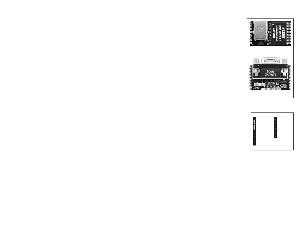
�HOST� INTERFACE� MODULE�
�The� ES� Master� Development� System� features� a�
�Host� Interface� socket,� which� allows� the� use� of�
�two� different� PC� interface� modules.� The� first� is� a�
�USB� interface� module� that� uses� a� standard� USB�
�cable� (not� included)� to� connect� to� a� PC’s� USB�
�port� or� a� USB� hub.� The� second� type� of� module�
�is� a� RS-232� interface� module� that� can� be�
�since� squelch� can� be� broken� by� unintended� interference.�
�To� get� a� better� idea� of� the� circuit’s� operation,� clip� an� oscilloscope� probe� on� both�
�RX� DATA� and� SQ.� DATA� (Squelch� Data).� With� the� transmitter� off,� the� SQ.� DATA�
�line� will� be� high� (which� means� that� the� output� is� squelched)� while� RX� DATA� will�
�be� switching� randomly.� Squelching� is� accomplished� by� comparing� RSSI� with� a�
�voltage� reference� created� by� R17� (potentiometer),� R18,� and� R21.� When� the�
�RSSI� falls� below� the� voltage� set� by� this� reference,� the� output� of� the� comparator�
�connected� to� a� standard� serial� COM� port� on� a�
�PC� using� a� straight-through� 9-pin� extension�
�cable� (not� included).� The� evaluation� board� is�
�considered� a� DCE� device� and� as� such� is�
�designed� to� be� connected� using� a� straight-thru�
�serial� extension� cable.� Do� not� use� a� null-modem�
�cable� as� the� boards� will� not� function.�
�USB� Interface� Module�
�Module� match.� The� USB� jack� or� the� D-sub�
�the� jumpers� on� the� header� as� shown� in� the�
�adjacent� figure.� This� routes� the� module's� data� lines�
�electrically� interfaced,� appropriate� protocol� must� be�
�employed� to� ensure� reliable� and� error-free� data�
�(U6)� will� pull� to� ground.� This� will� disable� the� data� slicer� created� with� the� additional�
�comparator� contained� within� U6.� It� may� be� helpful� to� refer� to� the� schematic�
�contained� later� in� this� document� in� order� to� better� understand� the� entire� function�
�of� this� circuit.�
�The� squelch� circuit� will� be� at� its� factory� default� setting� until� the� user� adjusts� it.�
�Remember� that� setting� a� higher� squelch� threshold� can� have� a� severe� impact� on�
�range.� The� squelch� level� affects� only� the� threshold� of� the� data� going� to� the� RS-�
�232� serial� port� and� the� SQ� DATA� line� on� TS2.�
�To� set� squelch,� verify� that� the� transmitter� is� off� and� turn� on� the� receiver.� Place�
�an� oscilloscope� probe� on� the� SQ� DATA� line,� and� adjust� R17� until� SQ� DATA�
�remains� high.� Two� resistors� (R27� and� R28)� are� used� to� connect� the� module� to�
�the� squelch� circuit.� These� may� be� removed� to� disconnect� the� squelch� circuit� and�
�prevent� it� from� slightly� loading� the� AUDIO� and� AUDIO� REF� lines.�
�USING� THE� ENCODER� AND� DECODER�
�The� MS� Series� encoder� and� decoder� use� a� 24-bit� address� to� provide� uniqueness�
�to� the� transmission� and� to� prevent� unintended� activation.� The� development�
�boards� come� with� a� default� address.� To� create� a� new� address,� press� and� hold�
�the� CREATE� button� on� the� transmitter� board.� The� address� is� randomized� for� as�
�long� as� the� button� is� held� down.� Once� released,� the� MODE_IND� LED� begins�
�flashing� to� indicate� that� the� encoder� is� ready� to� accept� Control� Permissions.�
�Press� the� Buzzer� and/or� Relay� buttons� to� indicate� to� the� encoder� that� they� will�
�be� used.� Press� the� Create� button� again� to� exit� Create� Mode,� or� let� the� encoder�
�time� out� after� 15� seconds.�
�On� the� decoder� board,� press� the� LEARN� button� and� the� MODE_IND� LED� begins�
�flashing� to� indicate� that� the� decoder� is� ready� to� learn� a� new� address.� Press� one�
�of� the� authorized� buttons� on� the� transmitter� board� to� send� a� signal.� Press� the�
�LEARN� button� again� to� exit� Learn� Mode,� or� let� the� decoder� time� out� after� 17�
�seconds� and� the� system� is� ready� for� use.�
�The� encoder� and� decoder� can� operate� on� one� of� four� different� baud� rates� as� set�
�by� the� Baud� Rate� Selector� switches.� A� faster� baud� rate� will� give� a� faster�
�response� time.� Please� see� the� encoder� or� decoder� data� guide� for� the� correct�
�settings.� If� the� switch� is� up� then� it� is� connected� to� Vcc,� if� it� is� down� then� it� is�
�connected� to� GND.�
�Page� 6�
�To� install,� select� the� module� to� be� used� and� then�
�line� up� the� pins� on� the� module� with� the� headers�
�on� the� board.� Verify� that� the� pin� one� polarity�
�marks� on� the� board� and� on� the� Host� Interface�
�RS232� Interface� Module�
�connector� should� face� away� from� the� board.� Figure� 5:� Host� Interface� Modules�
�Press� firmly� on� the� module� so� that� it� slides� fully�
�into� the� header.�
�The� development� system� may� be� prepared� for� host� T� S� 1� T� S� 2�
�operation� with� the� supplied� Linx� software� by� setting� PDN� ENC� S� Q.� DATA�
�TX� PDN� NC�
�PDN� R� S� 2� 3� 2� AUDIO� REF�
�TX� R� S� 2� 3� 2� AUDIO�
�TX� DATA� R� SS� I�
�to� the� Host� Interface� Module.� Despite� being� TX� ENCODER� RX� DATA�
�/CLK� RX� DECODER�
�/CLK� S� EL� RX� PDN�
�LO� V� DET�
�NC�
�transfer� since� the� ES� Series� modules� do� not� GND�
�encode� or� packetize� the� data� in� any� manner.� It� is� TX� RX�
�important� to� understand� that� the� development� Figure� 6:� Jumper� Configuration�
�boards� are� transparent;� that� is,� the� user's� software�
�is� entirely� responsible� for� controlling� the� timing� and� error� correction� aspects� of�
�the� link.� The� evaluation� boards� have� no� provision� to� check� or� qualify� the�
�incoming� data.� When� designing� a� protocol� to� transfer� data� across� a� wireless� link,�
�it� is� very� important� to� remember� that� interference� is� inevitable.� The� protocol� must�
�support� error� detection� and� correction� if� it� is� to� be� successful.� A� correctly�
�designed� protocol� will� provide� optimum� performance� and� throughput� for� product-�
�specific� applications� while� taking� into� account� the� timing� and� data-rate�
�requirements� of� the� module.� For� further� information� on� protocol� considerations�
�please� refer� to� Application� Note� AN-00160.�
�If� the� designer� needs� to� develop� protocols� using� a� physical� implementation� other�
�than� an� RS-232� or� USB� interface,� the� designer� can� build� the� custom� interface�
�circuitry� in� the� prototyping� area� and� route� the� module's� data� signals� from� the�
�header� to� the� prototyping� area.�
�Page� 7�
�发布紧急采购,3分钟左右您将得到回复。
相关PDF资料
MDEV-900-HP3-PPS-RS232
KIT MASTER 900MHZ HP-3 SIP RS232
MDEV-900-HP3-SPS-USB
KIT MASTER 900MHZ HP-3 USB SMD
MDEV-900-NT
TRM 900 NT MASTER DEV SYSTEM
MDEV-GPS-SG
KIT MASTER DEV GPS SG SERIES
MDEV-GPS-SR
KIT MASTER DEV GPS SR SERIES
MDEV-LICAL-HS-ES
KIT MASTER DEV HS ES RF MODULES
MDEV-USB-QS
KIT DEV MASTER USB QS SERIES
MF11-0010005
THERMISTOR NTC 100OHM -+5% PROBE
相关代理商/技术参数
MDEV-900-HP3-PPS-RS232
功能描述:KIT MASTER 900MHZ HP-3 SIP RS232 RoHS:否 类别:RF/IF 和 RFID >> RF 评估和开发套件,板 系列:HP3 标准包装:1 系列:- 类型:GPS 接收器 频率:1575MHz 适用于相关产品:- 已供物品:模块 其它名称:SER3796
MDEV-900HP3PPS-RS232
功能描述:射频开发工具 HP-3 Master Dev Sys Pinned, RS232 Module
RoHS:否 制造商:Taiyo Yuden 产品:Wireless Modules 类型:Wireless Audio 工具用于评估:WYSAAVDX7 频率: 工作电源电压:3.4 V to 5.5 V
MDEV-900-HP3-PPS-USB
功能描述:射频开发工具 HP-3 Master Dev Sys Pinned, USB Module
RoHS:否 制造商:Taiyo Yuden 产品:Wireless Modules 类型:Wireless Audio 工具用于评估:WYSAAVDX7 频率: 工作电源电压:3.4 V to 5.5 V
MDEV-900-HP3-SPS-RS232
功能描述:KIT MASTER 900MHZ HP-3 RS232 SMD RoHS:是 类别:RF/IF 和 RFID >> RF 评估和开发套件,板 系列:- 标准包装:1 系列:- 类型:GPS 接收器 频率:1575MHz 适用于相关产品:- 已供物品:模块 其它名称:SER3796
MDEV-900HP3SPS-RS232
功能描述:射频开发工具 HP-3 Master Dev Sys SMD, RS232 Module
RoHS:否 制造商:Taiyo Yuden 产品:Wireless Modules 类型:Wireless Audio 工具用于评估:WYSAAVDX7 频率: 工作电源电压:3.4 V to 5.5 V
MDEV-900-HP3-SPS-USB
功能描述:射频开发工具 HP-3 Master Dev Sys SMD, USB Module
RoHS:否 制造商:Taiyo Yuden 产品:Wireless Modules 类型:Wireless Audio 工具用于评估:WYSAAVDX7 频率: 工作电源电压:3.4 V to 5.5 V
MDEV-900-NT
功能描述:射频开发工具 NT Series Dev kit w/ Transparent module
RoHS:否 制造商:Taiyo Yuden 产品:Wireless Modules 类型:Wireless Audio 工具用于评估:WYSAAVDX7 频率: 工作电源电压:3.4 V to 5.5 V
MDEV-900-TT
制造商:Linx Technologies Inc 功能描述:TRM 900 TT MASTER DEV SYSTEM 制造商:Linx Technologies Inc 功能描述:RF Development Tools TT Series Master Development System